Accurate polishing processing of precision parts
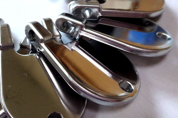
In precision parts used in the semiconductor and medical fields, there are many cases where cutting marks (cutter marks) cannot be tolerated even in machined parts.
In such cases, our company uses precision polishing to maintain the surface roughness (Ra around 1.0) while suppressing dimensional changes to almost zero (about 1 to several μm).
Precision polishing is a highly advanced process that requires skilled technology, but we have experience with many precision parts and can handle not only aluminum but also stainless steel and titanium.
It is especially used for semiconductors and medical/physiological equipment parts.
What is accurate polishing?
This is a processing technology that uses a special abrasive to polish the surface of parts by hand.
It depends on the material and condition of the material, but basically the polishing is done in stages: rough polishing (about #300), medium polishing (about #400 to #1,200), and final polishing (about #2,000).
With buffing, there are cases where the shape collapses or the dimensions change too much, but our precision polishing process can keep the dimensions and shape changes to a minimum.
The dimensional change is approximately 1 to 3 μm.
The standard finish is Ra0.4 to 0.8, and it is possible to achieve what is called a quasi-mirror finish.
It is mainly used for semiconductor manufacturing equipment parts, medical instruments, objects, and other artworks.
By performing precision polishing in-house, we have established a system to maintain the quality of the final product above a certain level.
Please try precision polishing for producing high value-added parts.
What is a cutter mark?
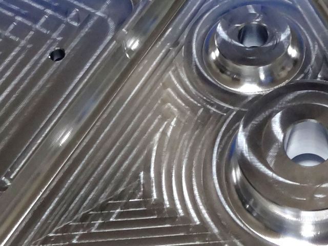
Many precision parts are manufactured by "cutting", which involves cutting the material by rotating a cutting tool called an end mill at high speed.
During cutting, a pattern called a cutter mark (or tool mark) is created as shown in the photo on the left.
These cutter marks are caused by the end mill moving along the part surface while changing its position.
Because minute differences occur, they remain as a pattern.
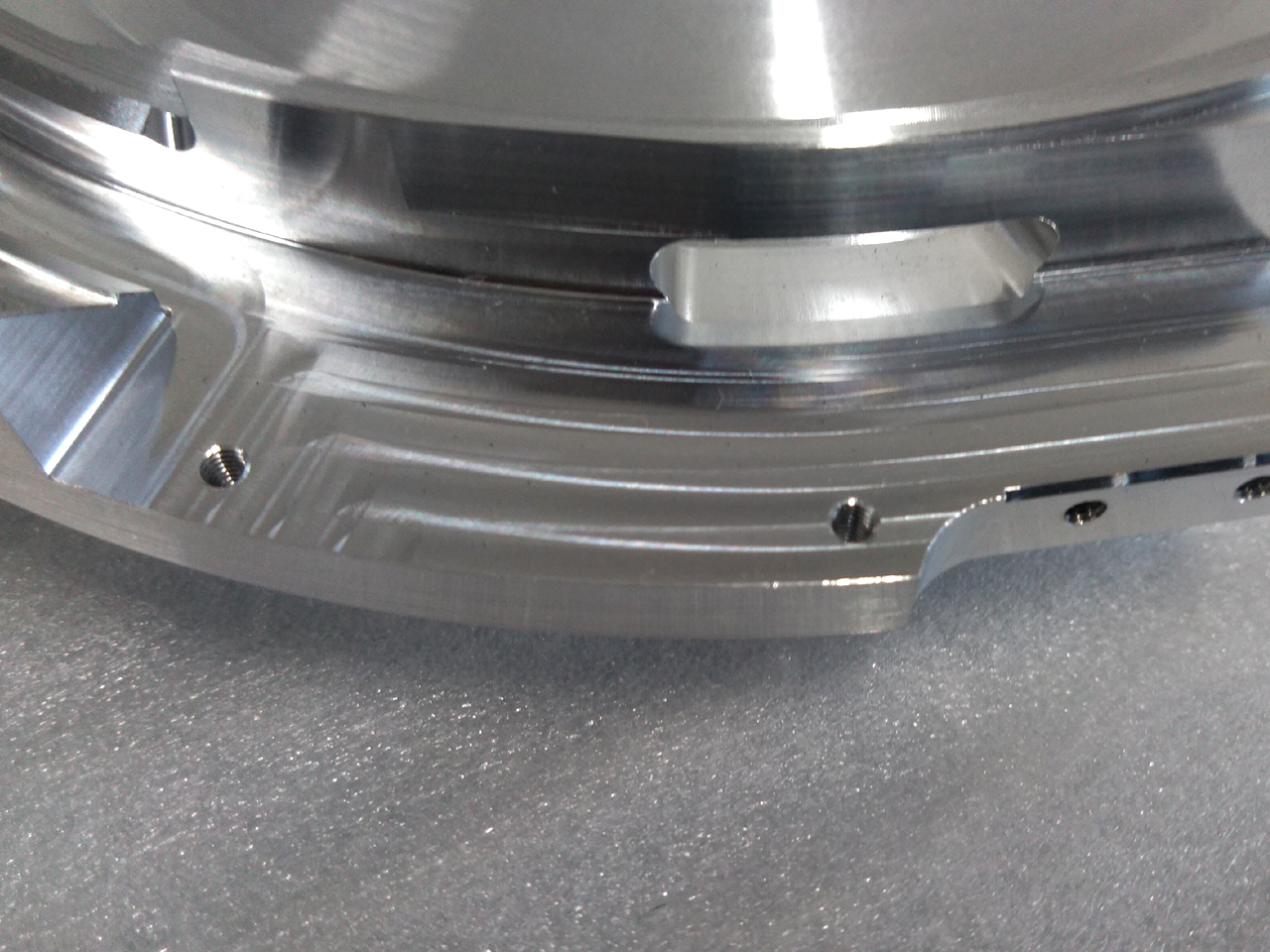
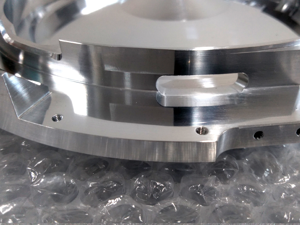
In the medical and semiconductor industries, as well as art works such as objects, polishing is required to remove these cutter marks while maintaining dimensional accuracy and sharp shapes.
At times like these, our wrapping processing comes into play.
The photo below shows the actual wrapping process. The left image is before wrapping, and the right image is after wrapping.
Before wrapping, cutter marks appear floating and the overall appearance is dull.
After wrapping, cutter marks are removed and the overall surface becomes glossy.
You can probably see the difference by clearly seeing the outline of the reflected shape.
The actual surface roughness is about Ra0.4-0.8μm.
Example

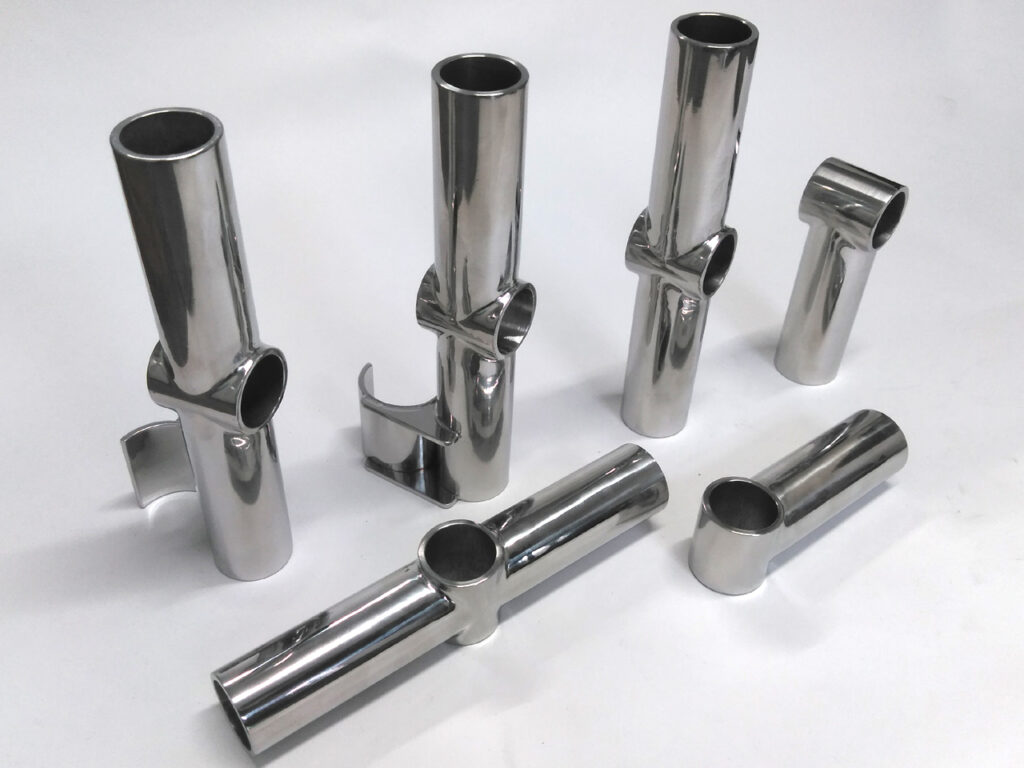
Medical device
Material: Stainless steel
This is a medical device manufactured using a complete cutting process.
Stainless steel cutter marks are very strong, so if you forcefully buff them, all the edges will sag and you won't be able to use it as a product.
The entire piece is precision polished to around Ra1.0.
Semiconductor manufacturing equipment parts
Material: stainless steel, titanium, aluminum
In semiconductor manufacturing equipment, cutter marks are said to have a negative effect on parts that come into contact with corrosive gases.
Because polishing is necessary to erase cutter marks while ensuring accuracy, our company basically uses lapping for semiconductor-related parts.
We have a lot of experience with important parts around wafers.
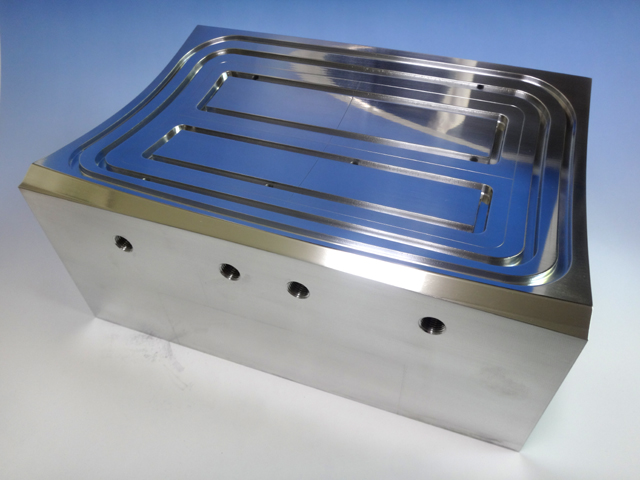
Vacuum component
A block for adsorbing resin molded parts.
The top surface is a free-form surface that matches the curved surface of the molded part, and a groove for vacuuming is dug perpendicular to that surface.
After all, wrapping is applied to improve adhesion to molded parts without losing its shape.